
■The outlines of COE formation and Research Achievements
1. Principle behind the COE
For more than twenty years, we have focused our attention on mainstream progress in silicon integrated circuit technology along with the world’s top-level research and developments in VLSI technology, which are seen to be the keys to the realization of an advanced information society. Building upon this solid foundation, the objectives of the COE are the development of fundamental technologies and new academic fields for a new integration system based on the design principles of both physical and information processing theory. We also plan to establish a novel, highly innovative system with advanced recognition/learning functions utilizing the integration of silicon Nano-devices, circuits, and architectures.
From an academic perspective, we aim to construct new fields of research by integrating circuit design and device processing technologies, currently disparate disciplines, using device modeling techniques as cross-linkers. It is important to educate many specialists with the critical abilities necessary to both research and develop a wide range of information and electronics-based academic fields. Such researchers will become future leaders in these new fields, which will produce a wide range of technological benefits from individual devices to entire systems. Therefore, we aim to foster and support promising individuals with the ability to approach technological challenges with a deep understanding and practical capability to facilitate the promotion of advanced independent research.
2. COE Objectives
2.1 Research Objectives
-Unification of silicon-based system, circuit, device-modeling and device-fabrication research.
-Solution of the persistent 3-diminsional-integration problems by a wireless integration methodology.
-Realization of integrated systems with high-level recognition and learning capabilities by innovative circuits and architectures.
2.2 Education Objectives
-Increase the number of doctoral students (10 students per year) and improve their quality.
3. COE member and Research subjects
3.1 Previous major achievements of the COE group
Over the past 30 years, our group has achieved top-level results in the following three fields in the area of research and education of silicon integrated circuits.
First, in the field of “Circuit and System Architecture,” Professor Iwata proposed the analog-digital fusion circuit architecture utilizing pulse modulation signals. He has developed a picture function associative processor, and demonstrated its technical functionality and high level of performance.
Professor Mattaushe has studied functional memory, devised an analog full-parallel comparison circuit, and developed analog-digital merged associative memory. Moreover, he has developed a multi-port memory circuit for parallel processing systems and successfully developed a test chip.
Professor Yokoyama proposed a photoelectron-fusion integration system with optical wiring. Students of the Research Center for Nano-devices and Systems assembled an image recognition test chip and demonstrated its basic operation.
Thus, our COE has top-level researchers in the fields of analog circuits, memory, digital circuits, and optical devices.
In the second field, that of “Device Modeling,” Professor Miura devised the MOS-transistor model HiSIM based on drift and diffusion physics. The HiSIM model has better accuracy than the BSIM model developed at UC Berkeley, which is the current global standard model, although the parameter counts of HiSIM are 1/5 or less. In addition, HiSIM has outstanding simulation function when advancing device segmentations, which can be used to estimate the high-frequency characteristics of the device without conducting any experiments. In January 2002, this model was released as free software and has been incorporated as a standard model into the simulators produced by almost all CAD vendors. We aim to replace BSIM and become the de facto standard in the next generation of CAD products.
In the third field, “Nano-device processors,” Professors Miyazaki and Sunami have successfully developed an experimental small-MOS transistor, and evaluated its properties, including its reliability. They have built and evaluated a detailed experimental device with a gate length of 30 nm and gate oxide thickness of 1.2 nm. Their research is competitive with the technology produced by the world’s top companies, a claim that other universities throughout the world cannot match.
Professor Kikkawa has studied the multilayer-interconnection system of integrated circuits and has developed technology to utilize materials with low dielectric constants. Moreover, this technology has been developed into wiring technology using electromagnetic waves or light.
3.2 Research fields and core members
Field I Circuits and system architecture
I-1. Radio frequency and analog circuits for wireless interconnections and signal processing
by Prof. A. Iwata & Assoc. Assoc. Prof. M. Sasaki
I-2. Associative-memory-based systems with recognition and learning capability
for image feature detection and recognition by Prof. H. J. Mattausch & Assoc. Prof. T. Koide
I-3. Processing system architecture with highly cognitive level by Prof. A. Iwata
Field II. Device Modeling
II-1 MOS device model for RF frequency range and SOI structure
by Prof. M. Miura-Mattausch & Res. Assoc. Dr. H. Ueno
II-2. Device model with RF and light response
by Prof. M. Miura-Mattausch & Res. Assoc. Dr. H. Ueno
Field III Nanodevices and Processes
III-1. Fundamental miniaturization techniques for Si-MOS transistors
by Assoc. Prof. K. Shibahara, and Prof. Miyazaki
III-2. Three-dimensional ultra-small SOI-MOS transistors
by Prof. H. Sunami & Prof. M. Miura-Mattausch
III-3. Functional nano-devices with multilayer dots:
by Prof. S. Miyazaki, Assoc. Prof. Higashi & Res. Assoc. Mr. H. Murakami
III-4. Integration technologies of wireless interconnect for chip-to-chip
by Prof. T. Kikkawa & Assoc. Prof. M. Sasaki)
III-5. Integration technologies of optical interconnection
by Prof. S. Yokoyama & Assoc. Prof. A. Nakajima
4. Formation of the COE
4.1 Basic Plan
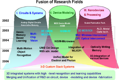
The objectives are investigated in parallel in three independent fields at the beginning, and merged a year after a year. Following are overview of our development plan:
2002- Extension of the worldwide top-level basic-technology position. Accelerated fusion of the research activities of the program’s three research pillars. Young program-member research proposals: Start of 2 cooperative projects on devices and modeling.
2003- Expansion of the cooperative research between the research fields. Promotion of research on wireless interconnects between chips. Young program-member research proposals: 2 additional cooperative projects between the device and circuit/system fields.
2004-Upgrading of the technology level in the light-interconnect and functional-memory fields to introduce them as new elementary technologies for integrated circuits.
2005- Highly efficient method for integrated device and circuit design. Basic 3-dimensional design technology for integrated circuit (vertical device) and electrical/optical integration.
2006- Establishment of the research-field organization and future-plan.
4.2 Progress of the COE
The research cooperation has started aiming at the fusion of the research fields. The researches for combining (1) high frequency MOS device modeling and RF circuit design, and (2) radio wave transmission system and integrated antenna structure have progressed. The researches on architecture utilizing wireless interconnection for associative memory based image processing, and bio-inspired visual processing have started. Furthermore, the research efforts on new devices and fabrication technologies for implementing 3 dimensional integration systems have also progressed.
For publicity of the concept of our COE, the 1st International Workshop on Nano-electronics was held in March, 2003. the 2nd International workshop was held in January, 2004, focusing on the device modeling.
In 2003, we have been awarded a large Grant in Aid for basic research (S) on “3 dimensional integration architecture using radio communication between chips for high recognition processing system”, and many other grants. COE members have also accomplished cooperative research projects cooperation with public laboratories and companies.
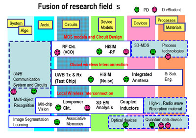
4.3 Three research fields are integrated to create new interdisciplinary fields.
HiSIM device modeling is situated between these three-research areas. At present, we are integrating these three research pillars to create new academic and technical fields of study.
The HiSIM model has been extended and is now applicable to the microwave frequency domain. Ongoing research at the COE will result in further extensions to light and electronic fusion device models. Our research fields will be united with this HiSIM device model as a major focal point. Currently, we are engaged in research into super high-frequency circuit design technologies utilizing the microwave HiSIM model and broadband wireless interconnections with low power dissipation. We are also studying the architecture of the vision system and algorithms for moving object recognition to establish a system with advanced recognition/learning capabilities.
In device processing by SOI, we have developed three-dimensional MOS devices, integrated antennas, integrated optical components, and optical sensor devices using quantum dot research.
Furthermore, the establishment of the base technologies of wireless and optical integration will allow us to address the problem of reconfigurable system integration with wireless interconnection technology.
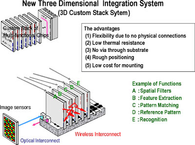
Currently, we are engaged in attempts to realize a three-dimensional integration system capable of interconnection between stacked multiple chips using electromagnetic waves. In this system, light interconnection will be used for long-distance connections between sensors.
This technology realizes (1) high level learning and recognition capabilities utilizing multi-chips, (2) image sensing capability of vision close to that of the human eye, and (3) flexible system configuration due to wireless interconnections.
As an example of such a system, the diagram shows the planned image recognition system consisting of multiple chips with various functions, including a spatial filter, feature extraction, and matching. New academic areas of interest include electromagnetic wave transmission theory in semiconductors, integration design techniques of integration antennas and circuits, and techniques for the integration of Ultra Wide Band communication technology.
4.4 New department in the graduate school of Advanced Sciences of Matters
An important aim of the COE is to bring-up a large number of young researchers, capable of doing self-defined and independent high-quality research, through the participation in leading-edge research programs of the COE. For this purpose, we established the new department of “Semiconductor Electronics and Integration Sciences”, in April 2004, in the Graduate School of Advanced Sciences of Matter, Hiroshima University. We have already developed the new program for high-level education through advanced research and practical training.
By extending graduate school education linked directly to advanced research, we intend to produce highly capable doctorate-level researchers who will make great contributions as future leaders in the fields of science and technology. Utilizing device fabrication equipment, such as the Super Clean Room and LSI Circuit Tester, we will foster the development of talented individuals with proven ability to perform valuable research in a wide range of fields, from devices to systems. A training program has been established to provide opportunities for high-level doctorate students to master not only advanced technology but also to develop a global point of view. Moreover, we have designed the new educational training program to further the development of logical thinking and planning abilities.
4.5 Establishment of research system for fusing research fields
The COE has advertised for postdoctoral COE researchers and employed 9 persons (3 foreigners) as additional core members of the COE in 2003. We also employ 6 doctoral course students as COE researchers.
We have set the research theme of each COE researcher on the boundary of existing research field in order to fuse the three research fields. We encourage co-operative research and free discussion between COE researchers. Our plan is to increase the COE researchers to 15 for postdoctoral researchers and to 16 for doctoral students in 2004.
5. Outline of research achievements
5.1 MOSFET Model: HiSIM for high frequency operation and the SOI structure has been developed. Its concept is to describe devices in accordance with basic physical principles. An 0.18um-CMOS testchip with RF-MOS devices and a voltage controlled oscillator (VCO) was designed and measured for evaluating the HiSIM model in the GHz frequency region.
5.2 Wireless Interconnection: Radio wave propagation through a silicon substrate was measured using integrated dipole antennas. A 20GHz radio wave propagates with low loss through a highly resistive Si substrate made by the proton implantation. This technology realizes the new 3 dimensional integration utilizing chip-to-chip wireless global interconnects for system clocks and buses for bi-directional data transfer and broadcasting.
Another complementary solution for wireless interconnects using resonant coupling of a spiral inductor pair was proposed. It realizes low power multi-giga bit/s wireless interconnects with highly parallel multi-channel communication suitable to transfer 2D data such as visions and neural information.
5.3 Associative memory based learning algorithm and integration of learning capability have been developed. It is applicable after image segmentation for various kinds of objects and recognition.
5.4 Multi-chip vision system architecture is proposed using PWM signals and wireless interconnection. Image recognition based on the Principal Component Analysis was also studied, and its applicability to multi-object recognition systems has been confirmed.
5.5 New MOS devices using new structures and materials, three dimensional MOS devices on SOI as well as, single metal-gate CMOS devices using the metal work function control are under investigation.
5.6 Optoelectronic merged technology:
The optical waveguides using EO materials were proposed for implementing an optical switch using resonance.
5.7 Functional nano-devices with multilayer dots
Floating gate devices with multi-layer quantum dot structure have been successively fabricated, and single electron charging behavior has been studied. Its application to a direct-optical-writing memory device is also proposed.
6. Future Plan
We have proposed the new concepts of chip-to-chip wireless interconnections, information processing architecture and new device technologies from the fused research fields. We will establish innovative basic technologies based on the concepts by simulation with theoretical models and experimental research by design and fabrication of proto-type systems. Through the advanced research, we will educate many doctoral researchers with the critical abilities necessary to both research and develop a wide range of information and electronics-based academic fields.
|