|
Profile |
|
|

| Name and Affiliation |

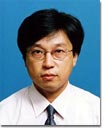
Anri Nakajima
nakajima sxsys.hiroshima-u.ac.jp sxsys.hiroshima-u.ac.jp
Hiroshima University, Research Center for Nanodevices and Systems
Associate Professor
|
| Education and Professional Background |
| 1991.3. |
ph. Dr received from Tohoku University, Graduate School of Science |
| 1991.5. |
Joined Fujitsu limited. He has been engaged in the research of Si quantum devices. |
| 1998.1. |
Associate Professor at Hiroshima University |
|
| Academic Societies |
Japan Society of Applied Physics, Physical Society of Japan |
| World Class Research Results |
・Si quantum dot formation with low-pressure chemical vapor deposition
・Room temperature operation of Si single-electron memory with self-aligned floating dot gate.
・ Formation of Sn nanocrystals in SiO2 film using low-energy ion implantation
・ Atomic-Layer Deposited Si-Nitride/SiO2 Stack Gate Dielectrics
・ Atomic-Layer Deposited Si-Nitride Gate Dielectrics |
| Pioneering Research Results |
・Si quantum dot formation with low-pressure chemical vapor deposition
・Room temperature operation of Si single-electron memory with self-aligned floating dot gate.
・ Formation of Sn nanocrystals in SiO2 film using low-energy ion implantation
・ Atomic-Layer Deposited Si-Nitride/SiO2 Stack Gate Dielectrics
・ Atomic-Layer Deposited Si-Nitride Gate Dielectrics
|
| Industrial and Nation-wide Cooperation |
Elpida Memory (from f.y. 2003), etc. |
| Important Publications |
| 1. |
A. Nakajima,
Y. Sugita, K. Kawamura, H. Tomita, and N. Yokoyama, "Si
quantum dot formation with
low-pressure chemical vapor deposition," Jpn.
J. Appl. Phys. Vol. 35, Part 2, No.2B, pp. L189-L191
(1996). (21 times) |
| 2. |
A. Nakajima, T. Futatsugi, K. Kosemura, T. Fukano, and N. Yokoyama, " Room temperature operation of Si single-electron memory with self-aligned floating dot gate," Appl. Phys. Lett. Vol. 70, No.13, pp. 1742-1744 (1997). (80 times) |
| 3. |
A. Nakajima, Q.D.M.
Khosru, T. Yoshimoto, and S. Yokoyama, "Atomic-layer-deposited
silicon-
nitride/SiO2 stack ---- a highly potential gate
dielectrics for advanced CMOS technology,"
Microelectronics Reliability Vol. 42, pp.1823-1835
(2002) (Introductory Invited). |
| 4. |
A. Nakajima, T. Itakura, S. Watanabe, and N. Nakayama, "Photoluminescence of porous Si, oxidized then deoxidized chemically," Appl. Phys. Lett. Vol. 61, No. 1, pp. 46-48 (1992). (75 times) |
| 5. |
T. Suemoto, K. Tanaka,
A. Nakajima, and T. Itakura, "Observation
of phonon structures in porous Si
luminescence," Phys. Rev. Lett. Vol. 70, No.23, pp. 3659-3662 (1993). (89 times) |
| |
(citation number at Feb. 13, 2004 on database of National Institute of Informatics) |
|
| Laboratory Page |
http://www.rcns.hiroshima-u.ac.jp/ |
| Personal Page |
http://www.rcns.hiroshima-u.ac.jp/nakajima/ |
|
|
|
|
|


