Mattausch, Hans Juergen 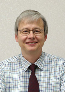
to Japanese Page
*Biography
Hans Juergen Mattausch was born in Hamm, Germany, in 1952. He received the Dipl. Phys. degree from the University of Dortmund, Dortmund, Germany, in 1977, and the Dr. rer. nat. degree from the University of Stuttgart, Stuttgart, Germany, in 1981.
In 1982 he joined the Research Laboratories of Siemens AG in Munich, Germany, where he was involved in the development of MOS technology as well as the design of memory and telecommunication circuits. From 1990 he led a research group on MOS-technology based power semicondutor devices, which included device design, modeling and packaging. In 1995 he joined the Siemens Semiconductor Group as Manager of the Department for Product Analysis and Improvement in the Chip Card IC Division.
Since 1996 he is with Hiroshima University, Higashi-Hiroshima, Japan, where he is presently a Professor at the Research Center for Nanodevices and Systems. His main present interest is in system design and architecture issues for effective utilization of nanodevices and nanotechnology.
*Academic Societies
The Institute of Electrical and Electronics Engineers Inc. (IEEE), USA
The Institute of Electronics, Information and Communication Engineers (IEICE), Japan
*Awards
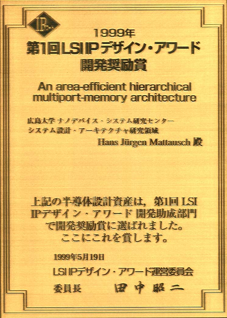
1999 LSI IP Design Award
Research result: An area-efficient multi-port memory architecture
The award is granted by the large Japanese semiconductor makers and others to honor Intellectual Property (IP) in the areas of circuit design, firmware, middleware or software, which is regarded necessary for the development of future systems on a chip.
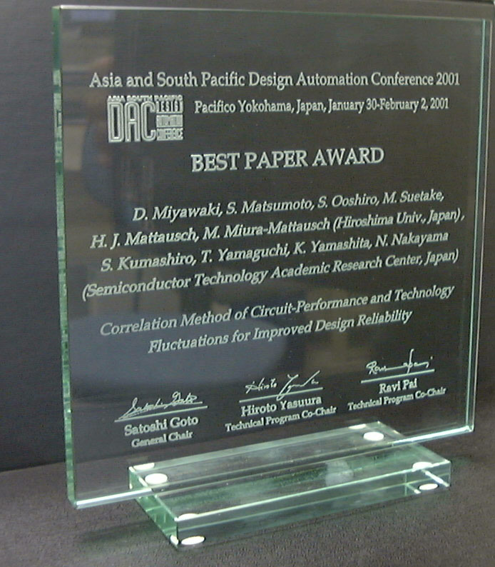
Best Paper Award of 2001 Asia and South Pacific Design Automation Conference
Paper Titel: Correlation Method of Circuit-Performance and Technology-Fluctuations for Improved Design Reliability
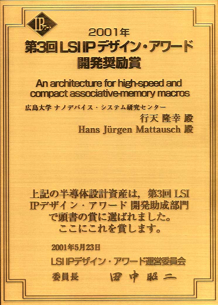
2001 LSI IP Design Award
Research result: An architecture for high-speed and compact associative-memory macros2002 LSI IP Design Award
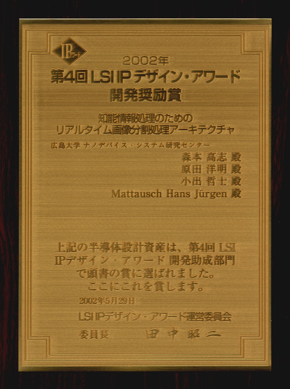
Research result: A real-time picture-segmentation archictecture for intelligent information processing2002 LSI IP Design Award
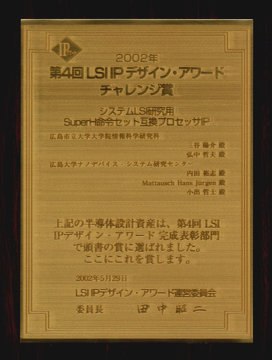
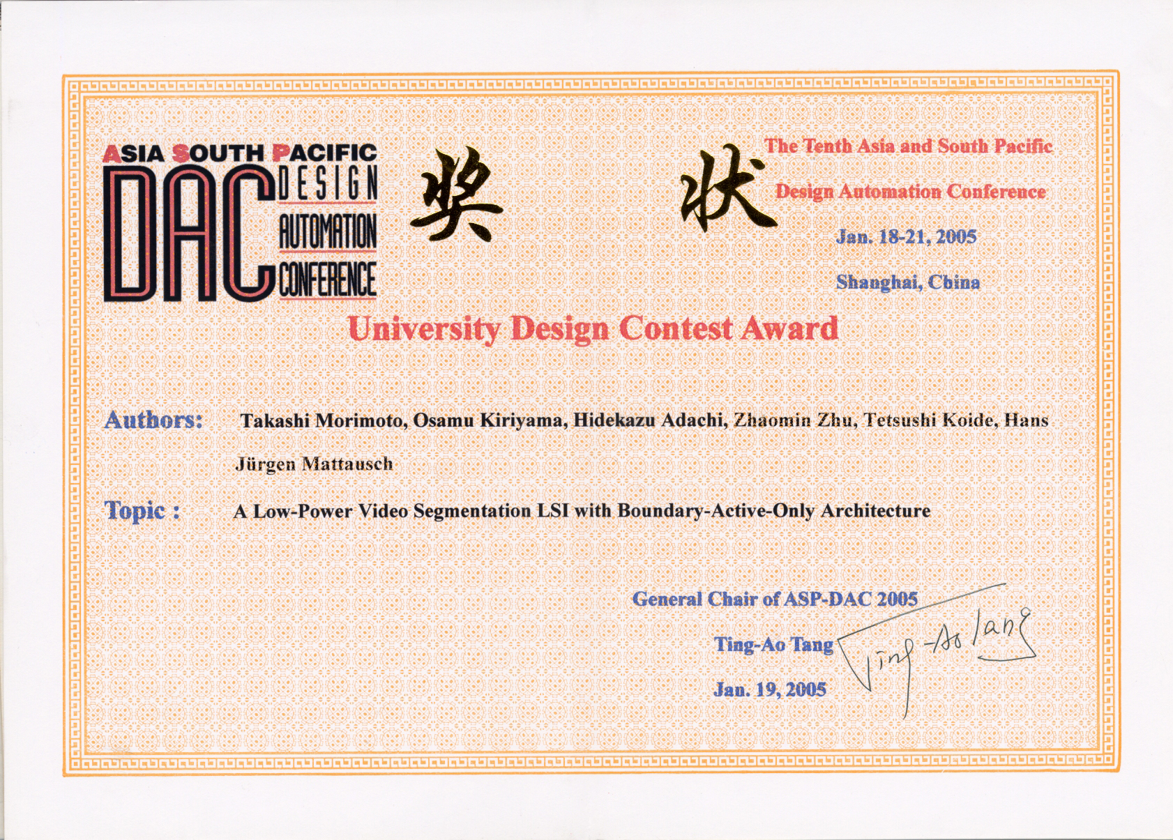
Research result: A mircoprocessor-core IP for system-LSI research with compatibility to the Super-H instruction setSpecial Feature Award of 2003 Asia and South Pacific Design Automation Conference, University Design Contest
Paper Titel: A Nearest-Hamming-Distance Search Memory with Fully Parallel Mixed Digital-Analog Match Circuitry2004 LSI IP Design Award
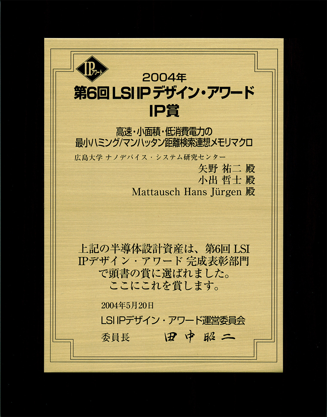
Research result: Area and power efficient associative-memory macro for fast nearest Hamming and Manhattan distance search2005 LSI IP Design Award
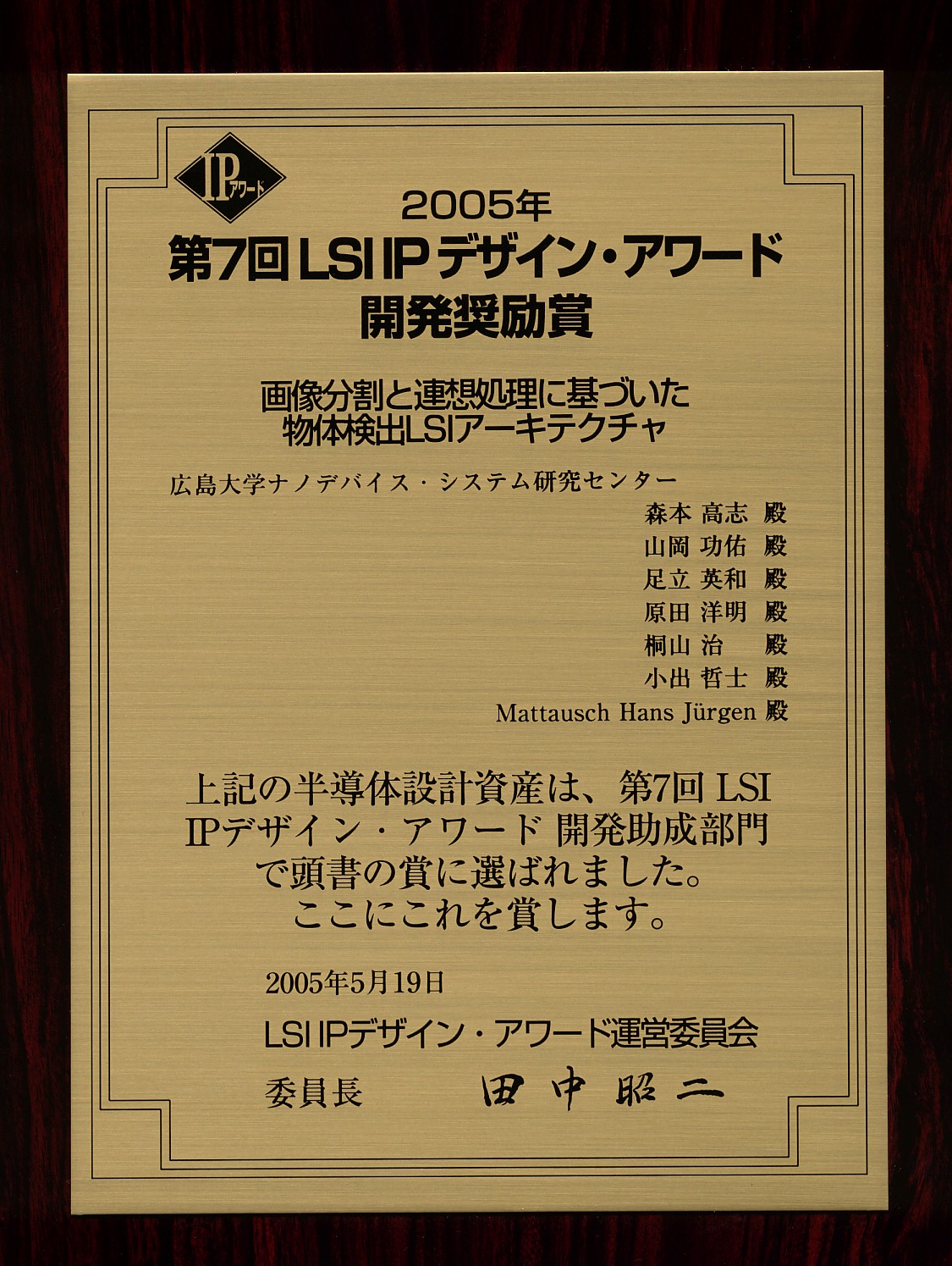
Research result: LSI architecture for object tracking based on image segmentation and pattern matchingUniversity Design Contest Award of 2005 Asia and South Pacific Design Automation Conference
Paper Titel: A Low-Power Video Segmentation LSI with Boundary-Active-Only Architecture2006 LSI IP Design Award
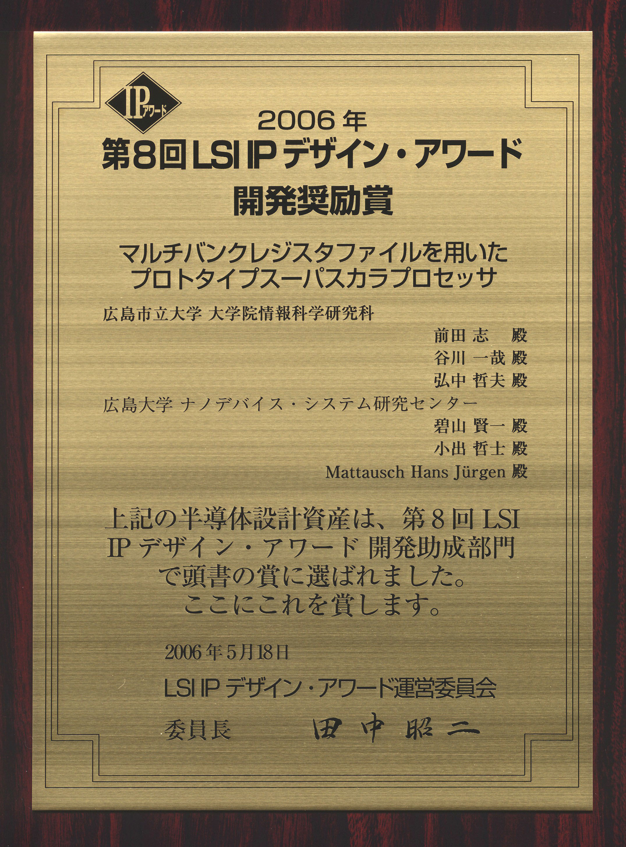
Research result: Prototype superscalar processor based on multi-bank registerfile2007 LSI IP Design Award
Research result: CAM-enhanced superparallel SIMD processor realizing fast pattern-matching functionality2008 LSI IP Design Award
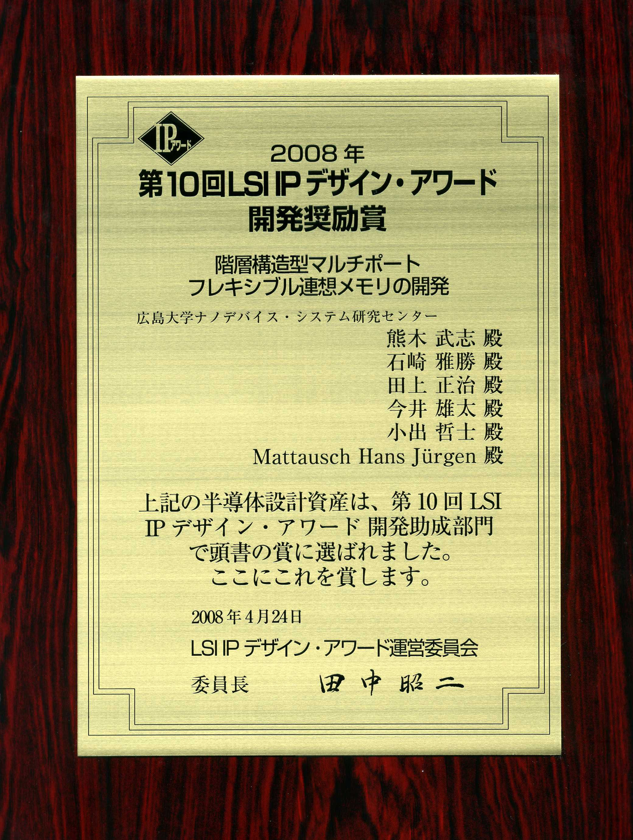
Research result: Flexible multi-port associative memory with hierarchical structure2010 Hiroshima University Intellectual Property Award for the Top 3 Researchers Registrations
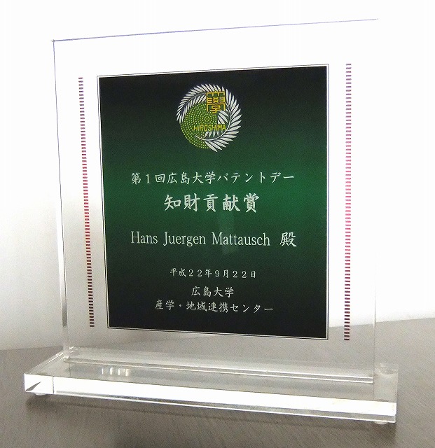
Research result: Hiroshima University Intellectual Property Award for the Top 3 Researchers with the Largest Number of Domestic Patent RegistrationsThe award was initiated 2010 for the purpose of honoring the researchers and faculty members of Hiroshima University who made the largest contribution to the university’s intellectual property portfolio.